Goal
Provide a high-gain, low-distortion, ultra-fast switching transistor by exploiting direct electromagnetic field energy (Poynting flow) instead of conventional electron current, thereby reducing noise and extending frequency response toward the optical region.
Problem
Conventional bipolar transistors suffer from electron-collision noise, limited switching speed, and restricted frequency response due to reliance on longitudinal electron current flow.
Concept Summary
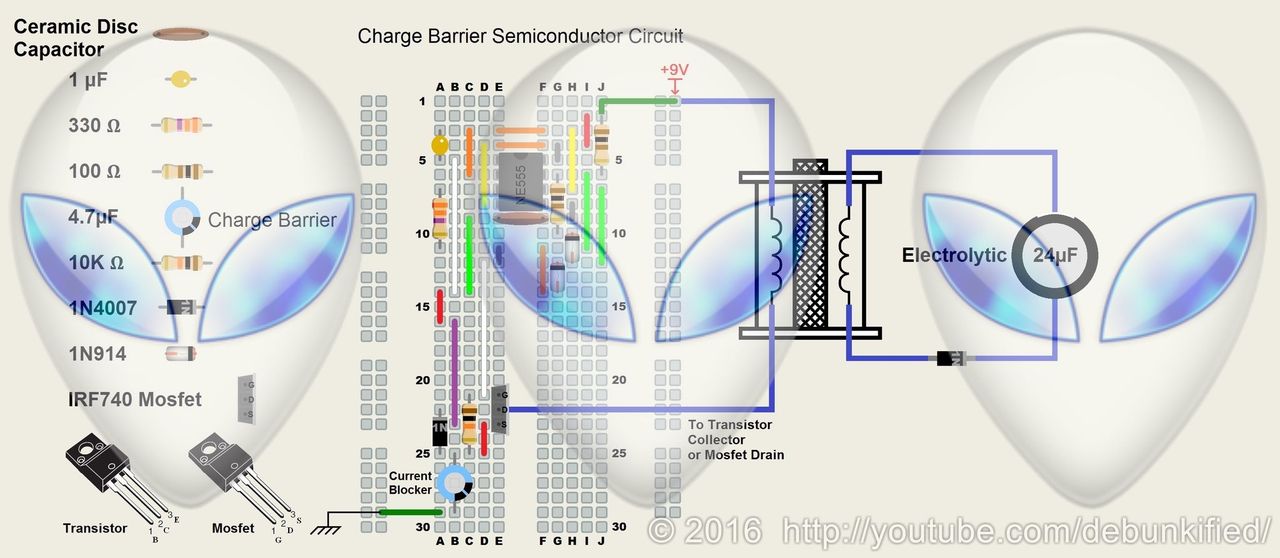
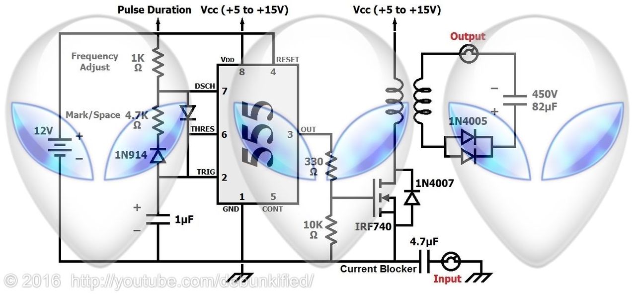
The Fogal Charged-Barrier Transistor integrates an electrolytic capacitor and a parallel bleed-off resistor into the emitter circuit of a bipolar transistor. The capacitor stores DC charge while the resistor allows a controlled bleed-off current that creates a high-frequency oscillating electromagnetic field (~=500 MHz). This field pins the emitter electrons, suppresses collision noise, and enables a Poynting-vector-driven energy flow that produces an AC supercurrent and spin-density-wave activity in the tantalum capacitor. The result is a device with high gain, low distortion, and an effective frequency response that can extend to the optical region.
Principles
- Poynting vector energy flow
- Spin-density-wave generation
- Charge-barrier electromagnetic pinning
- Electrolytic capacitor bleed-off oscillator
- AC supercurrent formation
Scientific Domains
Materials
- Tantalum electrolytic capacitor
- Bipolar silicon transistor
- Metal-film parallel resistor
- Silicon substrate
Mechanisms of Action
- Bleed-off resistor creates a small oscillating E-field on the capacitor plate
- Oscillating E-field generates a corresponding magnetic field (high-frequency)
- Pinned electrons in the emitter reduce collision noise
- Spin-density wave in the tantalum capacitor stores energy
- Poynting energy density flow transports energy across the crystal lattice
- Collapse of the DC field releases an AC supercurrent
Energy Sources
Applications
- High-speed low-noise amplifiers
- Optical-frequency communication devices
- Signal processing with reduced thermal noise
- Advanced switching circuits
Claimed Performance
High gain, low distortion, faster switching; frequency response up to the optical region; reduced electron-collision noise; generation of an AC supercurrent.
Experimental Evidence
Photographs from a Tektronix transistor curve tracer (microamp range) show high-frequency (~=500 MHz) oscillations, formation of a DC electromagnetic field, pinning of electrons, and discharge events consistent with an AC supercurrent and Poynting energy flow.
Limitations
- Device performance highly dependent on precise capacitor and resistor values
- No independent peer-reviewed replication reported
- Claims of optical-region operation lack quantitative verification
- Potential sensitivity to temperature and aging of electrolytic capacitor
Red Flags
- Unconventional claim of using field energy to bypass electron current without accepted theoretical support
- Absence of peer-reviewed data or independent replication
- Potential implication of over-unity or free-energy behavior