Palmer Craig: Hall Effect Device (Battery, rectifier,
amplifier)
 **[rexresearch.com](../index.htm)**
---
**Palmer H. CRAIG**
**Hall
Effect Device**
---
***Radio
World* (January 29, 1927), p. 11**
**"Tubeless Receiver Claimed by Professor,
Using Bismuth & Copper"**
by **Robert
Bangs**
**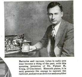**
Recently
it was announced at Mercer University (Macon GA), that the
Westinghouse Electric & manufacturing Co. had offered
Dr. Palmer H. Craig, head of the physics department of the
university, $100,000 for a new device which is supposed to
replace vacuum tubes as amplifiers and detectors.
The
device is called an "electromagnetic detector and amplifier"
and consists of a series of bismuth plates stacked in a pile
and interlaced with copper wires. The bismuth plates are
protected by a coating of sulfur because bismuth, a very
brittle substance, is likely to crumble.
**Long
Sought After**
Many
attempts have been made by various investigators to make use
in this manner of the this property of bismuth and of
similar properties of allied metals but so far there has
been no claim of success, until Dr. Craig came along. The
most common attempted application is to the rectification of
AC for filament and plate voltage supply. Lack of efficiency
and of dependability have been the main causes of failure.
Another limitation is the supply of suitable metals in
commercial quantity.
One
of the metals which displays similar properties is
molybdenum. This has been used by scientists of the Bureau
of Standards for converting light energy from the sun into
electricity.
**From
Earth To Sun!**
A
certain amount of success has been achieved and it seems
possible that power may soon be derived directly from the
sun in this manner. Here, also, lack of efficiency and of
adequate supply of the metal are limitations. There is
plenty of molybdenum to be had in different parts of the
world, but not all molybdenum is suitable for the purpose.
There seems to be an active component in the metal which is
responsible for the peculiar property, and it is now the aim
of the scientists to isolate this substance.
Apropos
the offer to Dr. Craig, Dr. Alfred N. Goldsmith, of the
Radio Corporation of America, denied that any such offer has
been made for Dr. Craigs device. Dr. Goldsmith, chief
broadcast engineer of the corporation, deprecates the idea
that the peculiar property of bismuth can be used for the
purpose claimed by Dr. Craig.
**He
is Not Yet Thirty**
Dr.
Craig emphasizes the point that the device will displace
batteries as well as vacuum tubes in radio sets.
Dr.
Craig, who is not yet 30, developed the invention, upon
which he immediately applied for a patent, for his thesis at
the University of Cincinnati where he received his degree of
Doctor of Philosophy last June.
When
asked to show the invention, Dr. Craig drew out a small
block of substance resembling sulfur. It was an inch thick,
about 3 inches long and 2 inches wide. Protruding from the
top were tiny wires. It was encased except for the top.
He
styled the device an application of bismuth plates as
detectors and amplifiers, which could be used in place of
present batteries and vacuum tubes in a radio.
**What
He Found Out**
In
his research for his Ph. D. degree at the University of
Cincinnati, Dr. Craig found that the bismuth plates might be
so used and the actual invention is described in part in his
doctors thesis.
The
inventor today spoke of the device as a series of about 10
thin bismuth plates, piled one on the other, with wires
running between them and finally on out to the actual radio
set.
Because
of the delicate nature of the bismuth plates, Dr. Craig has
protected them with a covering of sulfur. According to the
inventor, the bismuth plates will generate the energy
necessary to operate the radio and serve as a detector and
amplifier.
**Describes
Process**
The
process is described in the scientists thesis as follows:
"The
author is at present using this additive principle in an
application of the Hall effect to rectification of
alternating current, with a method similar to that described
by Descoudres.
"The
additive principle used in this connection produces a Hall
potential of several volts in low fields with thin bismuth
films, and thus gives the Hall effect a practical importance
as a rectifier, especially in radio and similar
applications."
---
***Physical
Review* 27: 772-778 (June 1926)**
**The Hall Effect in Bismuth with Low
Magnetic Fields**
by
**Palmer
C. Craig**
**Abstract
---** The Hall effect in bismuth for a magnetic field
strength of from 0.07 to 1.00 gauss was accurately
determined by improved methods. Production of the bismuth
films. Various methods for obtaining excessively thin,
homogenous bismuth films were tried and compared, such as
casting, electroplating, evaporating, sputtering, and
metallic spraying, of which the last three methods were
particularly successful. Measurement of very low voltages.
By refinements made in the potentiometer and measuring
circuits, reading to one-tenth microvolt were accurate and
reproducible. Magnitude of the Hall effect at low fields.
The value of the Hall coefficient, R, is abnormally large
between 0.07 and 0.30 gauss, having a value of -171 at 0.07
gauss, as compared with a value of -11 which R had for this
film at 15 gausses. The value at 4220 gausses was -29, A
curve is plotted showing the rapid decrease in the value of
-R between 0.07 and 0.30 gauss, and comparison is made with
higher values of field strength. It is noted that by putting
the Hall potential of one film in series with one or more
other films we obtain comparatively high values of the Hall
emf, which may be applied to great advantage as an
alternating current rectifier in radio and similar
applications.
**Introduction**
Since
the discovery of the Hall effect in 1875 much has been done
to elucidate this phenomenon both experimentally and
theoretically. But, with the exception of Righi (Ref. 1),
who employed fields comparable to that of the earth, and a
few others, almost all investigators have used strong
fields. It is important to know accurately the effect of low
fields, to compare it with the known facts and to determine
whether any abnormal relations exist. As the effect of the
magnetic field is small in all cases, a great refinement of
the potentiometer and measuring circuits is imperative with
weak fields, and the preparation of the bismuth strips
presents great difficulties and requires special methods.
**Preparation
-- Experimental Arrangements**
Since
the Hall effect increases with the thinness of the metallic
strips, the first requisite was to prepare extremely thin
films of metal. Bismuth and tellurium, which have the
highest Hall coefficient of the ordinary metals, were
selected and six different methods were tried in order to
find the best and quickest way of making films which would
be extremely thin and at the same time electrically
continuous. These processes were casting, dipping, spraying,
electroplating, and sputtering.
Thin
films of bismuth cannot be produced by casting unless
pressure is exerted on the surface of the metal as it cools,
and provision must then be made for lateral expansion when
solidifying.
Surprisingly
thin and uniform films were, however, obtained by dipping
mica sheets into molten bismuth and using the metallic film
which adhered to the mica. If the surface of the mica be
slightly roughened with hydrofluoric acid, and care be used
in withdrawing the mica from the molten metal, a very thin
and uniform film can be obtained by this very simple and
rapid method.
Much
work was done by the author to produce very thin plates of
bismuth and tellurium by the process of spraying molten
metal. Excellent results were obtained both with the
"Schoop" compressed air metallic spraying process, and also
with the "Gravitas" metal dust spraying process. Cooperation
in this part of the work was kindly rendered by the Metals
Coating Company of Philadelphia. Both of these spraying
processes involve spraying metals in the molten state by
means of a compressed air gun. In the case of bismuth it was
found advisable to use compressed nitrogen, instead of air,
in order to prevent oxidation of the sprayed layer. When
applied to mica, glass, and bakelite, excellent films of
both bismuth and tellurium were obtained.
Attempts
to produce homogenous films by electroplating met with poor
results, even when great care was used regarding
temperature, speed of the rotating cathode, and
concentration of solution.
Evaporation
of molten bismuth in a partial vacuum produced very good
results. Bismuth was placed inside an evacuated bell-jar and
was melted by an electric heater. A glass plate, suspended
above the arrangement, collected the evaporated bismuth in
the form of excellent films.
Cathodic
sputtering undoubtedly produces the thinnest films of any
method. With reasonable care bismuth films can easily be
prepared by this method so thin as to be quite transparent.
Sputtering was accomplished by applying the secondary
current of a 20,000 volt transformer to anode and cathode
electrodes placed inside a bell-jar evacuated to 30 microns.
Rectification of the secondary current by a kenetron
accelerated the action. A disc of bismuth 3.5 inches in
diameter was used as a cathode, and the glass plate on which
the film was to be sputtered was placed just outside the
Crookes dark space, which was about 2 cm long. With a
current of 5 milliamperes excellent films were produced on
glass in about 20 minutes.
**Disposition
of the Apparatus**
The
very weak magnetic films employed in this work were obtained
from an air core solenoid. When a given current is passed
through such a coil the field at the center is easily
calculated. This calculated value was checked by a
calibrated ballistic galvanometer in conjunction with a flip
coil. The actual coil employed consisted of 100 turns of
wire wound on a rectangular wooden form 8 x 11 cm in
cross-sectional area, the size of this form being just large
enough to accommodate the film used. The inductance of this
coil was 2.5 millihenries, and it was therefore necessary to
pass 35.2 milliamperes through it in order to get a field of
one gauss at the center. Because of the extremely low values
of the magnetic field used, it was necessary to shield the
arrangement carefully from any action of the earths and
stray fields. Several methods were tried to accomplish this
shielding, the one finally adopted being that of placing the
set-up so that the plane of the bismuth field coincided
exactly with the magnetic inclination of the earths field
at that point, thus eliminating any magnetic component in a
direction perpendicular to the plane of the magnetic film.
Care was taken to keep all iron away from the vicinity of
the apparatus, and upon actual measurement stray fields were
found to be negligible.
Chemically
pure bismuth for producing the films was furnished by Eimer
and Amend and the film itself, obtained by any one of the
previously described methods, was mounted on bakelite with
sodium silicate as a binder. Contact at the ends for the
longitudinal current was made by phosphor-bronze spring
clips, and contact at the edges of the film, for picking up
the transverse Hall potential, was obtained by means of
small brass fingers attached to machine screws passed
through the bakelite. The surface of the film was carefully
cleaned with weak hydrochloric acid solution to remove
surface oxides, and the entire film and connections were
then painted with sodium silicate to keep semi-conducting
layers of dirt and moisture from collecting on the surface
of the film. In some cases it was even found advisable to
mould the entire arrangement in sulfur to obviate this
difficulty.
Since
the potential differences to be measured were of the order
of one microvolt, extreme care was taken to render the
measuring apparatus very accurate and stable. The transverse
Hall effect potential was measured by means of a Leeds and
Northrup type K potentiometer, redesigned with a system of
calibrated external shunts which increased the sensitivity
of the instrument 10 times. Four galvanometers of varying
degrees of sensitivity were used with potentiometer for null
readings, the most sensitive galvanometer having a
sensitivity of 12.2 mm per MV. The longitudinal current
through the film was supplied by large storage cells, the
output of which passed through a large filter system of two
very large inductances in series with the line, the lines
being shunted by two condensers of 6 microfarads each. This
filter eliminated erratic action caused by sudden
fluctuations of the longitudinal current occasioned by
bubbling of the cells.
The
main current through the potentiometer itself was passed
through a similar filter and was allowed to flow overnight
before taking readings so that greater stability could be
expected. The null potentiometer reading on the standard
cell was checked before and after and after each
measurement.
Greater
care was taken to eliminate all spurious effects. Thermal
effects, of course, construed the greater part of these
corrections. Junctions of dissimilar metals in the circuit
were reduced to a minimum, and the remaining potentials due
to Thomson and allied effects were accurately measured the
instant the longitudinal current was broken. Grounding one
side of the potentiometer circuit was found to increase
stability.
For
the work at high magnetic fields, a large electromagnet was
used. This magnet was capable of producing a field of 18,000
gausses in a narrow air gap, the field of which was measured
by a calibrated ballistic galvanometer in conjunction with a
flip coil.
**Experimental
Results & Discussion**
Using
a bismuth film obtained by metallic spraying, 3.5 x 8.0 cm
in area and 0.012 cm thick, the results shown in Table I
were obtained. These results are in agreement with those
obtained with films of the other type described previously.
In this table three different ranges of magnetic field
strength were investigated with the same bismuth film and
under the same general conditions. A longitudinal current of
1.5 amperes was used throughout Table I. The "residual" emf
(measured in microvolt) which is referred to in the second
column is the potential difference caused by the fact that
the brass fingers which pick up the transverse Hall
potential cannot possibly be placed at exact equipotential
spots with regard to the longitudinal current. These
contacts were placed as near to equipotential points as
possible and the remaining difference of potential was
measured as given in the second column of the table. The
second and third columns automatically include the sum of
the thermal effects, since it is of course impossible to
eliminate the thermal potentials from the potentials
indicated in these columns. However, the spurious effects
are eliminated when column two is subtracted from column
three in order to get the net Hall emf in the fourth column.
The Hall coefficient, R, given in the fifth column is
calculated from the usual formula (Ref. 2),
R =
Ed / IH ,
Where
R is the Hall coefficient, d the thickness of the film in
centimeters, i the longitudinal current in abamperes, H the
magnetic field strength in gausses, and E the net Hall emf.
**Figure
1:** Relation between Hall coefficient, -R and the
magnetic field strength for the Hall effect in bismuth
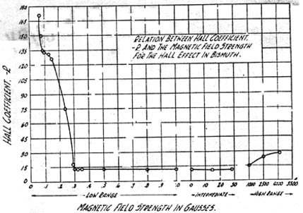
It is
immediately apparent that the Hall coefficient is abnormally
high in the range of very low fields, and falls rapidly in
value as the field is slightly increased. Reference to the
graph (Figure 1) shows a slight irregularity near 0.1 gauss,
a straightening out of the curve at about 0.3 gauss, and
then an approximately linear relation until a field strength
of 1.0 gauss is reached. Reading s in an intermediate range
of zero to 30 gauss showed that -R is practically constant
at a value of 10.27 which Von Ettingshausen and Nernst found
for bismuth at a field of 1650 gausses. In the range from
1000 to 4200 gausses the coefficient increases slightly from
15 to 29. This curve was selected from a dozen similar
graphs as being one of the most representative, and the
irregularity in the neighborhood of 0.1 gauss is typical of
similar irregularities in all curves obtained with the
various films.
These
results show that the value of -R at very low fields is
higher than has been heretofore suspected and that the curve
for -R, plotted against field strength, shows a marked rise
in this low range.
Each
of the values in Table I are average values for
approximately 12 readings at each value of field strength.
These readings are reproducible to approximately one-tenth
of a microvolt, and the readings forming the averages did
not vary more than this amount.
**Table
I:** Hall effect in bismuth for low, intermediate and
high fields
Gausses
Residual emf Residual + Hall
emf Net Hall
emf -R
0.07
14.0 microV 15.5
microV
1.5
microV
171
0.08
14.1
15.6
1.5
150
0.09
14.2
15.7
1.5
135
0.10
14.2
15.8
1.6
133
0.13
14.4
16.1
1.7
131
0.15
14.3
16.9
2.6
126
0.24
14.0
16.3
2.3
75
0.29
14.6
21.1
6.5
18
0.30
14.5
19.8
5.3
14
0.32
14.4
19.6
5.2
13
0.35
14.8
20.5
5.7
13
0.50
14.6
22.7
8.1
13
0.80
14.6
26.6
12.0
12
1.00
14.6
29.6
15.0
12
1.0
14.5
29.5
15.0
12
15.0
14.3
35.1
20.8
11
28.5
14.4
60.4
46.0
11
1000
14.0
1889.0
1875.0
15
2500
14.0
7514.0
7500.0
24
4220
14.0
15324.0
15310.0
29
During
the course of the experiments an interesting incidental fact
was discovered, namely that the Hall effect of one film may
be put in series with that of one or more other films, the
sum of these series potentials agreeing very well with the
calculated sum of the Hall potentials of the individual
films as observed separately. Although this fact has little
application where quantitative readings of a high degree of
accuracy are desired, it is of real importance in any
application where larger values of Hall potential are
desirable than those which can be obtained with a single
film. The author is at present using this additive principle
in an application of the Hall effect to rectification of
alternating current with a method similar to that described
by Descoudres (Ref. 4). The additive principle used in this
connection produces a Hall potential of several volts in low
fields with thin bismuth films, and thus gives the Hall
effect a practical importance as a rectifier, especially in
radio and similar applications. Work on the additive
principle is also being done by Sarek (Ref 5).
The
results here presented indicate that there is considerable
work to be done in further investigating abnormalities in
the Hall coefficient at very low fields, and also suggest
that certain modifications or explanations will have to be
introduced into the theory of the Hall effect to account for
the interesting changes in the Hall coefficient at low
fields.
In
conclusion, the author wishes to acknowledge his
indebtedness to Dr. Louis T. More, Dr. R.C., Gowdy, and Sr.
S.J.M. Allen for their kind help and valuable advice
tendered throughout the progress of the work.
Ref.
1 ~ Righi: Journale d. Physique 3: 127 (1884)
Ref. 2 ~ L.L. Campbell: "Galvanomagnetic &
Thermomagnetic Effects", p. 9
Ref. 3 ~ Von Ettinghausen & Nernst: Wied. Ann. 29: 343
(1886)
Ref. 4 ~ Des Coudres: Phys. Zeitschrift 2: 586 (1901)
Ref. 5 ~ Sarek: Eleck. U. Maschinenbau 43: 172 (1925)
---
**U.S. Patent 1,822,129**
(Sept. 8, 1931)
**System & Apparatus Employing the Hall
Effect**
**Palmer H.
Craig**
My
invention relates broadly to electrical apparatus for
modifying the behavior of electrical current and more
particularly an apparatus for effectively employing the
transverse potential difference in certain metallic plates
when subjected to the action of a longitudinal current and
the influence of a magnetic field.
One
of the objects of my invention is to provide a device
consisting of a plurality of rectangular metallic foil
sheets or metallic alloy plates in stacked arrangement
insulated one from another and electrically connected in
parallel at opposite ends thereof and in series along the
transverse axis thereof, whereby current of direct
current characteristic may be secured in a circuit which
connects to points along the transverse axes of the plates
when alternating current is supplied to the opposite end of
the plates and a magnetic field created around the plates.
Another
object of my invention is to provide a construction of fixed
rectifier for alternating current which remains in permanent
adjustment and does not require resetting from time to time.
Another
object of my invention is to provide a device for modifying
electrical current of alternating characteristic for
rectifying, amplifying, or causing the generation of
electrical oscillations of any selected frequency.
Still
another object of my invention is to provide an electrical
apparatus particularly adapted for operation in conjunction
with the circuits of a radio receiving system for rendering
feeble signal currents observable.
A still further object of my invention is to provide an
apparatus unit which may be connected in circuit with
electron tube apparatus for facilitating the operation of
the electron tube apparatus in the reception of signaling
energy.
Other
and further objects of my invention will be understood from
the specification hereinafter following by reference to the
accompanying drawings in which:
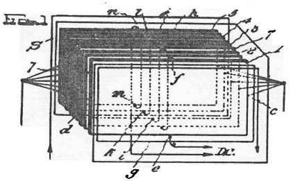
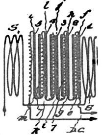
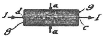
Figure
1 represents in perspective view the arrangement of parts in
the apparatus of my invention; Figure 2 is an end view of
the apparatus showing more clearly the direction of the
magnetic field perpendicular to the plane of the metallic
plates; Figure 3 is a schematic view showing the arrangement
of the metallic films which comprise the apparatus of my
invention; Figure 4 is a diagrammatic view showing the
wiring arrangement of the apparatus of my invention when
used as a rectifier; Figure 5 shows one of the applications
of my invention in a reflex signaling receiving circuit;
Figure 6 illustrates an application of my invention as a
detector in a radio circuit; Figure 7 shows a circuit
arrangement which makes use of the principles of my
invention in the amplification of signal energy, provision
being made for facilitating the production of oscillations;
Figure 8 shows a circuit arrangement wherein the
longitudinal current which passes through the plates of the
apparatus of my invention is derived from a source
independent of the source which creates the magnetic field
about the plates; Figure 9 illustrates a circuit arrangement
employing a plurality of the devices of my invention as an
amplifier of incoming signaling energy and as a rectifier of
the amplified energy; and Figure 10 shows the fundamental
arrangement of the magnetic field transverse to the plane of
several metallic plates in the apparatus for developing the
principles set forth herein.
**Figure
1:**
**Figure
2:**
**Figure
3:**
**Figure
4:**
**Figure
5:**
**Figure
6:**
**Figure
7:**
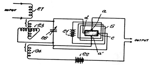
**Figure
8:**
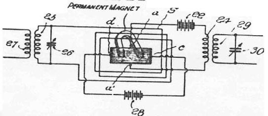
**Figure
9:**
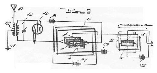
**Figure
10:**
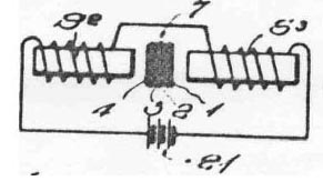
My
invention makes use of the "Hall", "Corbino" and similar
electromagnetic phenomena for the rectification or
amplification of alternating currents, and the generation of
sustained electrical oscillations in electrical circuits.
The
"Hall" effect consists, briefly, of an electromagnetic
phenomenon observable when a strip or film of metal carrying
a longitudinal current I, (Figure 3) is placed in a magnetic
field perpendicular to the plane of such a strip, a
transverse potential difference being set up between the
edges a, a, of the strip, this difference of potential
being approximately, under normal condition represented by
the formula:
E =
HI/d
Where
E = the transverse potential difference;
I = the current (longitudinal) through the strip;
d = the thickness of the strip;
H = the magnetic field strength
The
"Corbino" effect is similar to the "Hall" effect, wherein a
radial current through a circular disc subjected to a
magnetic field perpendicular to the plane of the disc,
produces a "circular" current through the disc.
I
have discovered that if plates or films of metal such as
bismuth, tellurium, bismuth-antimony alloy, or other metal
or alloy, be connected as shown in the drawings, the devices
will act as a practical electrical rectifier of impressed
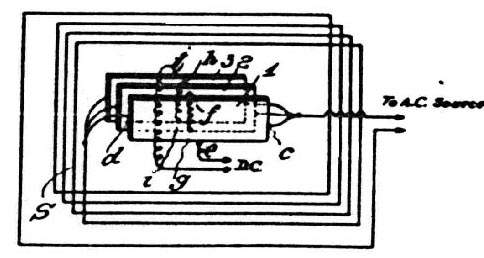
alternating currents. Refering to the drawings in Figure 4,
the alternating current is sent through the strip 1 from c
to d, in one-half of the cycle, and from d it enters the
solenoid S, being an air-core or a core of magnetic
material, thence after passing through the solenoid it
returns to the alternating current source. In the other half
of the cycle the operation is, of course, reversed.
Figure
4 also shows the method of stacking many plates 1,2 and 3 on
top of one another, with suitable insulation between, and
then connecting the positive "Hall" effect potential point
of one plate to the negative "Hall" effect potential point
of the one below, as represented in the drawings at e, f, g,
h, i, and j. In other words, the transverse potential of all
the plates 1,2 and 3 are put in series in order to add up to
larger values of potential than would be obtained with a
single plate.
It is
obvious, that since the polarity of the "Hall" effect
potential difference changes in synchronism with either the
change in polarity of the points c and d, or with the change
in direction of the magnetic flux through the plate, the
polarity of the point e, j (Figure 4) will always be the
same with respect to each other when both the magnetic flux
and also the longitudinal current through the plates change
in phase synchronously with each other, The arrangement
shown in Figure 4 will then obviously give a pulsating
direct current at the point e, j.
The
construction of the apparatus of my invention is more
clearly illustrated in Figure 1 where the metallic films
have been represented at 1, 2, 3, 4 and 5 separated by
insulated sheets 7. Opposite ends of the films are tapped as
represented at c and d. The transverse axes of the films are
connected in series as represented at e, f ,g, h, i, j, k,
l, m, and n for delivering a direct current. The end view of
the apparatus in Figure 2 shows more clearly the arrangement
of the films and the dielectric sheets. The solenoid winding
has been divided into two sections for producing a
transverse magnetic field through the metallic films.
In
Figure 3 I have shown a stacked arrangement of metallic
films separated by insulated sheets in accordance with my
invention, where the alternating current I passes along the
longitudinal axes of the films from d to c. I provide copper
end contacts 8 and 9 which bridge all of the metallic films
enabling the films to be connected in the electrical circuit
in parallel. The point contacts across the transverse axes
of the films have been represented at a and a.
The
device may be used as a rectifier in ordinary electrical
circuits where the power drawn from the rectifier is of
sufficiently low value as to render the method practicable.
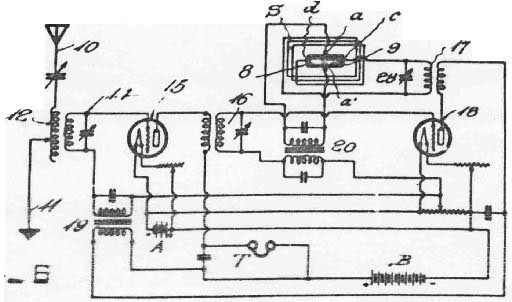
The arrangement can also be used as a rectifier in radio
transmitters and receivers, especially to replace the
crystal detector or the triode vacuum tube detector in radio
reception. It could be used either alone or in combination
with electron tubes, a typical circuit diagram of the latter
method being given in Figure 5.
Referring
to Figure 5 in more detail the receiving antenna system is
represented at 10 which connects to a ground system at 11
with a coupling inductance 12 therein coupled to the tuned
input circuit 14 of the electron tube 15 which functions as
a radio frequency amplifier. The output of the radio
frequency amplification circuit 16 with the input circuit of
a second stage of radio frequency amplification constituted
by electron tube 18, the output circuit of which includes
transformer system 17tuned as represented at 28 for
supplying exciting current to solenoid S through a series
circuit which passes through the longitudinal axes of the
metallic films from points d to c. A direct current is
derived across the points of contact a and a which is
directly proportional to the incoming signaling energy. The
rectified current is delivered through a transformer system
20 to the input circuit of the electron tube 18 which also
functions as an audio frequency amplification system
delivering its audio frequency output through transformer 19
with the input circuit of electron tube 15 which serves also
to amplify at audio frequency delivering its output to
telephones T. Battery A supplies filament heating current
for the several tubes while battery B supplies space current
for the tubes. The tuned system 17-28 permits a relatively
large value of current to pass through the metallic films
and thereby secure maximum direct current energy across the
transverse axes of the metallic films. My invention may be
applied to all standard circuits as well as to the reflex
system of Figure 5.
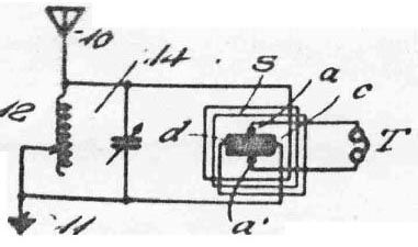
Referring
to Figure 6 a simplified circuit as illustrated showing the
application of the principle of my invention to a simple
radio receiving apparatus. In this circuit the incoming
signaling energy delivered from tuned circuit 14 passes
through the longitudinal axes of the metallic films from d
to c at the same time setting up a magnetic field by means
of solenoid S for deriving direct current across the
transverse axes of the metallic films at a and a
proportionate to the incoming signal energy. This direct
current directly actuates the telephone responsive device T.
It
should be noted that, due to the fact that this system is a
perfect rectifier (that is, it admits of no inverse
potential or currents in the output) it will produce no
distortion in the reproduction of radio telephone signals
and voice, and is, therefore, far superior to either the
crystal detector or the electron tube from the standpoint of
faithful reproduction, in addition to its superior qualities
of stability, ease of operation and lower cost of
maintenance.
Figure
7 illustrates a circuit arrangement which I employ in the
amplification of signaling energy by means of the apparatus
of my invention. An input circuit has been illustrated in
the form of an inductive coupler 25 tuned by variable
condensor 26 and connected through the longitudinal axes of
the metallic films at d and c. A permanent magnetic field
may be established about the metallic films by means of a
local source 21 connected in circuit with the winding S. An
iron core may be provided for this solenoid S. Incoming
signaling energy is supplied through winding 27 coupled with
the windings 25. The transverse axes of the films at a and
a are connected in series with a local source 22, and an
inductance 24 which couples with the inductance system 25. A
desired degree of regenerative amplification is thus
introduced for increasing the amplitude of the impulses of
signaling energy delivered to the output circuit. The
principle of my invention may be applied to an oscillator
where the input coil 27 connects to a small local exciter of
alternating current and the output connected through a
transformer system. By employing selected values of
inductance, capacity and resistance the system may be
arranged to oscillate at either audio or radio frequencies.
Figure
8 illustrates a method of obtaining greater energy
amplification in the apparatus of my invention. A permanent
magnetic flux is set up through the thickness of the plates
and also a permanent longitudinal current is established
along the horizontal axes of the plates from a battery 28. A
tuned input circuit system 27-25-26 is arranged to excite
the winding s which encloses the stack of alternately
positioned films and dielectric sheets. The longitudinal
axes of the films are connected at points a and a with an
output circuit including a source of potential 22, and
inductance 24. The inductance 24 is inductively coupled to
an inductance 29 tuned by means of condensor 30 in the
output circuit of the electrical system. The fluctuating
magnetic field from the winding S which varies in proportion
to the amplitude of the signaling energy is superimposed on
the permanent field which is established.
The
input may also be superimposed on the longitudinal current
instead of upon the magnetic field. The local battery for
supplying longitudinal current to the conductive field may
thus be eliminated. The local battery 22 in the circuit of
the electrical system is provided to boost the voltage of
the output to a proper value for the operation of the
succeeding amplifier stages or the reproducing unit, the
"Hall" fluctuating potential being then superimposed upon
this steady potential. By increasing the number of
conductive films in parallel the effective potential may
also be increased.
In
Figure 9 I have shown an application of my invention to an
electron tube circuit where the conductive films have their
longitudinal axes connected in series in the output circuit
of electron tube 15. A constant magnetic field is supplied
from battery 21 to the winding S. In this manner the device
operates as a radio frequency amplifier, delivering
amplified energy to an output circuit across the transverse
axes of the conductive films in series as represented at e
and j, the output circuit including battery 22 and solenoid
winding S. The solenoid winding S connects in series with
the longitudinal axes of conductive films as represented at
c and d and across the transverse axes at a and a I
connect the output circuit which includes the battery 22.
The arrangement of the conductive films within the solenoid
winding S serves as a rectifier of amplified energy
delivered by the conductive films within the solenoidal
winding S.
Figure
10 shows a method I may employ for setting up the magnetic
field which threads through the conductive films. A pair of
compressed silicon steel filing cores or other suitable
magnetic material or alloys are arranged on opposite sides
of the stack of alternately positioned conductive films and
dielectric sheets. On these coils are provide the windings
S2 and S3 supplied from the local source 21. The stack of
bismuth or metallic alloy conductive films may be quite
thick but the magnetic field is concentrically normal to the
plane of the conductive films. The magnetic field in some
cases is produced by a solenoidal coil of approximately 1000
turns on cores of compressed silicon steel filings. The
resultant transverse pulsating direct current is several
volts for only one milliampere flowing through the field
coil and longitudinally through the conductive films in
parallel. I have found that where four amperes alternating
current at 60 cycle frequency is passed through a 12 turn
coil and then through the conductive films connected in
parallel with themselves longitudinally, the resulting
pulsating direct current component across each conductive
films is approximately 50 microvolts. When the conductive
films above referred to are connected in series transversely
200 microvolts may be obtained. The values obtainable may
readily be used in the operation of electron tubes. The
arrangement of the apparatus is such that connections may be
readily made with electron tube circuits as represented at
Figure 9 without their interposition of transformer systems.
When
an iron core is used with the device of my invention with
the proper permeability curve an asymmetric characteristic
curve may be obtained with the device similar to that
obtained with a triode tube. This ability of the device of
my invention facilitates the generation of self-oscillations
in the device. The device when properly connected will,
therefore, operate as an amplifier or as an oscillator in
addition to its properties as a rectifier.
While
I have described my invention in certain preferred
embodiments, I desire that it be understood that various
modifications may be made without departing from the spirit
of the appended claims.
---
Other
U.S. Patents by Palmer Craig:
U.S.
Patent 1,778,796 -- : System & Apparatus Employing the
Hall Effect
U.S. Patent 1,825,855 -- System & Apparatus Employing
the Hall Effect
Hall effect device having anisotropic lead conductors --
US3197651A
ELECTRIC REGULATOR -- CA386489 (A)
HALL EFFECT AND SIMILAR ELECTRICAL PHENOMENUM TO RADIO, ETC.
-- CA296979
VOLTAGE REGULATOR -- CA456916 (A)
Storage battery cap with gas recombining means -- US2615062
Electrical measuring instrument -- US1778795 (A)
System and apparatus employing the hall effect -- US1778796
(A)
Photoelectric electronic tube -- US2296269 (A)
System and apparatus employing the "hall effect" --
US1825855 (A)
System for suppressing interfering currents --
US1792001 (A)
Ultra-violet lamp and system -- US1798658 (A)
Method and means for cooling glass walled bodies --
US2357727 (A)
Electromechanical connection -- US2327622 (A)
Frequency modulation radio receiver -- US2310304 (A)
Method of preserving fruits, vegetables, etc. -- US1981583
(A)
Radio receiving system -- US1935738 (A)
Television system -- US2444221 (A)
Photoelectric apparatus -- US2414636 (A)
Static suppressor system -- US1956121 (A)
Electronic tube and control therefor --US2435202 (A)
Gaseous discharge device -- US2405089 (A)
Oxygen enrichment system for gas engines -- US2444222 (A)
Power control circuits -- US2001836 (A)
Magnetic amplifier -- US2937351 (A)
Ultra high frequency oscillator -- US2520383
Television system -- US2393890
Hermetically-sealed storage battery with gas recombining
means -- US2465202 (A)
Regulator system -- US1992146 (A)
Power control circuits -- US2001838 (A)
Crystal filter system -- US2463249 (A)
Power control circuits -- US2001837 (A)
Process of making magnetic amplifiers -- US3008882 (A)
---
http://news.google.com/newspapers?nid=999&dat=19270402&id=rqM8AAAAIBAJ&sjid=YfYFAAAAIBAJ&pg=3035,3721219
Bismuth-coated Device Is Invented by
Youthful Georgian Student
No
Batteries, No Tubes In New Set... the invention of Dr.
Palmer Craig, youthful head of the depart ment of physics at
Mercer ...
---
http://books.google.com/books?id=micDAAAAMBAJ&pg=PA59&lpg=PA59&dq=Palmer+Craig+bismuth&source=bl&ots=1WEoPhyIoa&sig=TtiVLGT76VhErxAnEn-4EStRWJk&hl=en#v=onepage&q=Palmer%20Craig%20bismuth&f=false
Popular Science - May 1927
... with this amazing invention of Dr. Palmer H. Craig, of
Cincinnati. Bismuth plates, it is said, generate the energy
to operate the radio set, and serve as detector ...
---
http://gradworks.umi.com/DP/15/DP15709.html
The Hall effect with low
magnetic fields
by
Craig, Palmer H., Ph.D., UNIVERSITY OF CINCINNATI, 1926, 8
pages; DP15709
Abstract: The Hall Effect in bismuth for a magnetic field
strength of from 0.07 to 1.00 gauss was accurately
determined by improved methods. Production of the bismuth
films. Various methods for obtaining excessively thin,
homogeneous bismuth films were tried and compared, such as
casting, electroplating, evaporating, sputtering, and
metallic spraying, of which the last three methods were
particularly successful. Measurement of very low voltages.
By refinements made in the potentiometer and measuring
circuits readings to one-tenth microvolt were accurate and
reproducible. Magnitude of the Hall Effect at low fields. A
curve is plotted showing the rapid decrease in the value of
-R between 0.07 and 0.30 gauss, and comparison is made with
the higher values of field strength. It is noted that by
putting the Hall potential of one film in series with one or
more other films we obtain comparatively high values of the
Hall e. m. f. which may be applied to great advantage as an
alternating current rectifier in radio and similar
applications.
---
http://prola.aps.org/abstract/PR/v29/i2/p332\_1http://adsabs.harvard.edu/abs/1927PhRv...29..332H
Physical Review, vol. 29, Issue
2, pp. 332-336
The Hall Effect in Bismuth with
Small Magnetic Fields
Heaps, C. W.
The Hall coefficient for a bismuth plate of dimensions
0.011x0.9x2.0 cm has been measured for magnetic fields
ranging from 0.07 to 2.40 gauss. The average value of the
Hall coefficient, R, in this range was 11.5, and variations
of R due to change of field strength in this range were less
than experimental errors. For larger fields the Hall
coefficient of this specimen decreased from 13.5 for a field
of 650 gauss to 5.9 for a field of 8600. It is concluded
that for similar ranges of field the data reported by Palmer
H. Craig are erroneous, probably because of insulation
leakage or uncompensated thermomagnetic effects. A simple
method of making very thin bismuth plates is described.
---
**https://journals.aps.org/pr/abstract/10.1103/PhysRev.30.964 **Phys. Rev. 30, 964 Published 1 December 1927**
Hall Effect in Bismuth with Low Magnetic Fields
Palmer H. Phys. Rev. 30, 964 Published 1 December 1927**
---
**https://journals.aps.org/pr/abstract/10.1103/PhysRev.27.772****The Hall Effect in Bismuth with Low Magnetic Fields****Palmer H. Craig****Phys. Rev. 27, 772 1 June 1926**
DOI:https://doi.org/10.1103/PhysRev.27.772
---
**https://ui.adsabs.harvard.edu/abs/1927PhRv...29..332H/abstract**
**The Hall Effect in Bismuth with Small Magnetic
Fields****Heaps, C. W**.
Abstract
The Hall coefficient for a bismuth plate of dimensions
0.011x0.9x2.0 cm has been measured for magnetic fields
ranging from 0.07 to 2.40 gauss. The average value of the
Hall coefficient, R, in this range was 11.5, and variations
of R due to change of field strength in this range were less
than experimental errors. For larger fields the Hall
coefficient of this specimen decreased from 13.5 for a field
of 650 gauss to 5.9 for a field of 8600. It is concluded
that for similar ranges of field the data reported by Palmer
H. Craig are erroneous, probably because of insulation
leakage or uncompensated thermomagnetic effects. A simple
method of making very thin bismuth plates is described.
Physical Review February 1927
DOI: 10.1103/PhysRev.29.332
---
**https://www.pinterest.com/pin/hall-effect-device-by-palmer-craig--616782111480165864/****Hall Effect Device by Palmer CRAIG**
Hall Effect Device and Free energy: "Tubeless Receiver
Claimed by Professor, Using Bismuth & Copper"; System
& Apparatus Employing...
---
**https://typeset.io/papers/the-hall-effect-in-bismuth-with-small-magnetic-fields-h781i2i5d4**
About: This article is published in Physical Review. The
article was published on 01 Feb 1927. The article focuses on
the topics: Quantum Hall effect & Thermal Hall effect.
The abstract of the paper titled "The Hall Effect in Bismuth
with Small Magnetic Fields" provides a concise summary of
the research findings regarding the Hall effect in bismuth
under varying magnetic field strengths. Here are the key
points explained:
Measurement of Hall Coefficient: The
study involved measuring the Hall coefficient (R) for a
bismuth plate with specific dimensions (0.011 X 0.9 X 2.0
cm) across a range of magnetic fields from 0.07 to 2.40
gauss. The Hall coefficient is a parameter that quantifies
the Hall effect, which is the generation of a voltage
difference across an electrical conductor when a magnetic
field is applied perpendicular to the current flow.
Average Value of Hall Coefficient: The
average value of the Hall coefficient obtained in this small
magnetic field range was found to be 11.5. Importantly, the
variations in R due to changes in field strength within this
range were less than the experimental errors, indicating a
stable measurement process
[ 1 ]
Behavior at Larger Fields: The abstract
notes that as the magnetic field strength increased beyond
650 gauss, the Hall coefficient decreased significantly,
dropping from 13.5 at 650 gauss to 5.9 at 8600 gauss. This
suggests that the Hall effect in bismuth behaves differently
at higher magnetic fields compared to lower ones.
Critique of Previous Work: The authors
conclude that previous data reported by Palmer H. Craig are
likely erroneous. They attribute these discrepancies to
potential issues such as insulation leakage or uncompensated
thermomagnetic effects, which could have affected Craig's
measurements. The authors emphasize the importance of
eliminating such errors to ensure accurate results
[ 2 ]
Method for Thin Bismuth Plates: The
abstract also briefly mentions a simple method for creating
very thin bismuth plates, which is relevant for conducting
the experiments accurately.
In summary, the abstract highlights the main findings of the
research, including the measured Hall coefficient values,
the behavior of the Hall effect under varying magnetic
fields, and a critique of previous studies, all while
introducing a method for preparing the bismuth samples used
in the experiments.
Quickly ask these questions
1. What method was used for R measurement?
2. How were experimental errors assessed in study?
3. What implications arise from Craig's erroneous data?
2 Sources
1The Hall coefficient for a bismuth plate of dimensions
0.011 X0.9X2.0 cm has been measured for magnetic fields
ranging from 0.07 to 2.40 gauss. The average value of the
Hall coefficient, R, in this range was 11.5, and variations
of R due to change of field strength in this range were less
than experimental errors. For larger fields the Hall
coefficient of this specimen decreased from 13.5 for a field
of 650 gauss to 5.9 for a field of 8600. It is concluded
that for similar ranges of field the data reported by Palmer
H. Craig are erroneous, probably because of insulation
leakage or uncompensated thermomagnetic effects. A simple
method of making very thin bismuth plates is described.
2It is also possible that the lack of agreement of Craig's
results with those reported in the present paper is due to
his not having eliminated thermomagnetic effects Campbell,
'Galvanomagnetic and Thermomagnetic Effects,' p Craig, Phys.
Rev It appears probable that Craig's results are incorrect
because of imperfect insulation of his apparatus. He states
that the stability of his system was increased by grounding
his potentiometer. There should, however, be no instability
which could be corrected in this fashion unless leaks of
variable resistance are present. It appears probable that
Craig's results are incorrect because of imperfect
insulation of his apparatus. It is also possible that the
lack of agreement of Craig's results with those reported in
the present paper is due to his not having eliminated
thermomagnetic effects To eliminate errors of this kind it
is often sufficient to reverse the direction of the magnetic
field and calculate the mean of the Hall e.m.f. 's for the
two directions of field. The thermal effect is thus averaged
out, since it does not reverse with the field while the Hall
e.m.f. does. Craig appears to have been very careful about
mounting his specimen but does not mention any special
precautions taken to keep his electrical circuits insulated
from each other. Also, he states that ''potentials due to
Thomson and allied effects were accurately measured the
instant the longitudinal current was broken,'-however, he
apparently did not test for the effect of the field on these
potentials. Furthermore, it does not appear in his paper
that spurious temperature effects were averaged out by
reversing the magnetic field. The Hall coefficient for
bismuth for small fields, with a primary current of 1.3
amps. Each value of R recorded above is the average of at
least five values. These five values for any one field
differed among themselves by about as much as the different
values of R in the table. Apparently the change of R for a
range of magnetic field from 2.4 to 0.07 gauss is no greater
than the errors of the experiment. Craig found R increasing
by a factor of more than 10 in this same range. TT IS a well
known fact that the coefficient of the Hall effect for
ordinary cast bismuth increases as the magnetic field is
diminished.1 Recently Palmer H. Craig has reported2
surprisingly large values of this Hall coefficient when
magnetic fields smaller than about 0.3 gauss were used, and
he suggests that modifications will have to be made in the
theory of the Hall effect in order to account for his
results. There are already several other phenomena connected
with the Hall effect which theories have not explained; the
genuineness of this new phenomenon should therefore be very
thoroughly established. Because of the possibility of these
sources of error in Craig's work the writer has made some
measurements of the Hall coefficient in weak magnetic fields
and has not found the abnormal values reported by Craig.
Manipulation of the plate was not difficult because it was
rather tightly adherent to the glass upon which it was
formed. Hence, it was possible by carefully scraping the
edge of the plate to adjust the Hall electrodes so that they
were quite accurately on an equipotential surface when the
primary current flowed and there was no magnetic field. A
thin plate of bismuth (listed by Eimer and Amend as c.p.)
was made by the following method. A glass tube with one end
drawn down slightly was clamped vertically and a bismuth rod
inserted. The rod was prevented from slipping out of the
bottom by the slight constriction there. About 10 cm below
the end of the tube was placed a clean, horizontal glass
plate. The lower end of the glass tube was now heated with a
small flame till the bismuth melted and a single large drop
was allowed to fall on the glass plate below. By a little
practice in adjusting temperatures and distance of fall very
thin, uniform, circular films of metal can be produced on
the glass plate in this way. The sensitiveness of the
apparatus was such that turning the plate over so as to
reverse the earth's field gave a deflection of 24 mm. The
table gives a set of results obtained for small magnetic
fields. The Hall electrodes were connected through a
potentiometer to a galvanometer of resistance 16.6 ohms and
sensitivity 17.3 mm per microvolt. The primary current
electrodes were connected through an ammeter and rheostat to
a 6-volt storage cell. The galvanometer circuit and the
primary current circuit were insulated from the earth and
from each other by ebonite,-except, of course, where
interconnection occurred in the bismuth plate. For the sake
of thermal insulation a thick coat of paraffin was put over
the plate and over the junctions of all wires leading to it,
and a layer of cotton was wrapped around the whole assembly.
It was then mounted, with ebonite insulation, on a stand
arranged with a graduated circle so that the specimen could
be rotated about a horizontal axis in the plane of the plate
and parallel to its length. Measurements were made as
follows. The galvanometer readings were noted in quick
succession for the field in one direction, for the field
reversed, and for the field in the original direction. The
reading for the reversed field was subtracted from the
average of the first and third readings and the difference
divided by two. The result gave the deflection due to the
Hall effect for the field used, and errors due to slow drift
of the galvanometer were eliminated. The corresponding
e.m.f. was calculated from the known sensitivity of the
instrument. This method is quick and accurate, and it gives
the same result as the potentiometer method provided the
potential drop in the specimen due to the galvanometer
current is negligible compared with the Hall e.m.f. 3 The
potentiometer in the galvanometer circuit was used for
balancing small thermal e.m.f . 's and for obtaining the
sensitivity of the galvanometer. To test the effect of
electric leaks one side of the potentiometer was connected
by a wire to the slate bench on which the apparatus was
disposed. Craig states that such a connection in his
apparatus was found to increase stability, so presumably he
used it in his work. It introduces a leak to ground in the
galvanometer circuit. Another wire was next used to connect
the enamelled iron tube of the. rheostat in the primary
current circuit to the floating side of the reversing switch
in the circuit of the Helmholtz coils. No particular care
had been taken to insulate these coils from the slate table
top, and the 6-volt storage battery used for exciting the
coils was standing directly on the tile floor supporting the
table. This second wire thus served as a leak from the
primary current circuit to ground, and the effectiveness of
the leak was altered by closing the reversing switch.
---
**https://www.usni.org/magazines/proceedings/1927/august/discussion****August 1927 Proceedings Vol. 53/8/294****Concerning the "Hall Effect Principle as applied to
Radio****by Dr. Craig**
(See page 482, April, 1927, Proceedings)
Lieutenant Harry F. Breckel, U.S.N.R.In the interest of the
service the writer wishes to offer the below mentioned
comment on the practical value of the Hall Effect Theory as
applied to rectification and radio usage by Dr. Palmer H.
Craig who conceived the modern application of a long
discarded principle. Not wishing to deprecate in any way the
work of Dr. Craig in applying the principle to modern radio
uses, nor wishing to discourage those working on it in the
future, yet the writer wishes to state that experiments
conducted do not bear out the claims as regards the
displacement of vacuum tubes by the device nor the
elimination of the usual current supply devices for the
modern radio receptor.
In his capacity as consultant in the commercial field of
radio, the writer had occasion to thoroughly investigate the
merits of the device and the claims of Dr. Craig in his own
laboratory at Macon, Georgia, and also in the laboratory of
a large commercial concern, the experiments being under
supervision of the inventor, and being conducted with a view
of purchase of the rights under his pending patents, if the
device proved of merit.
The experiments conducted decisively proved that, insofar as
the present conception of the device utilizing the Hall
Effect Principle was concerned, the apparent rectifying
effect produced in connection with an alternating current
was that brought about by purely thermal junction effects
caused by lead and copper being in contact with the bismuth
films, and which when heated slightly by the current flowing
through them had the effect of producing a uni-directional
transverse current. This current, however, was very small,
being of the order of a few millivolts, efficiency of the
device being very low when output was checked against input.
The effect was not true Hall Effect, in which application,
the currents and voltages are of very small values, in fact
to quote a professor of physics of a certain university,
the limitations of the Hall Effect Theory as applied
practically make virtually impossible the obtaining of any
currents of sufficient amplitude to be of any value.
It was further found that the current and voltage values
obtained during the conducting of the experiments were also
largely due to inductive effects due to wires leading to the
meters being in the strong magnetic field in which the
bismuth plates were placed to secure the Hall Effect
action. It was found that the meters themselves were
influenced by close proximity to the field. These current
readings could be obtained without the use of the bismuth
plates, but when the meters were removed to a distance which
precluded their being acted on inductively, the readings
fell to absolute zero. Thus this definitely disproved the
claim to rectification by the device. Insofar as the
application to radio reception was concerned, the results
were zero, it being considered that such effects as were
obtained were due purely to capacity effects, the plates as
assembled being nothing more than a condenser and feeding
through the initial antenna current through this action to
the ordinary vacuum tubes of the receiver. It is significant
that the device was never utilized alone, but was always
used in connection with vacuum tubes of conventional design
which really did the work.
By and large therefore, the Hall Effect Theory as
applied practically to radio usage is considered to be
entirely without merit at this time, although, of course, it
may be that the far distant future may see it made useful in
this direction. The inventor is still working hard on the
device with the usual optimism and persistency of the
researcher, and it is sincerely hoped that Dr. Craig, who is
a good friend of the writer, will ultimately achieve a very
much deserved success, although as mentioned, the practical
merits of the Hall Effect Principle would seem to place an
insurmountable barrier in his path.
---
Patents re: Bismuth Film
JP2011221048
Also published as: US2011244224
PROBLEM TO BE SOLVED: To provide anti-reflection coating for
infrared ray having excellent adhesion to chalcogenide glass
and excellent weather resistance. ;
SOLUTION: An anti-reflection coating 13 is provided on a
surface of a substrate 12 made of so-called chalcogenide
glass containing sulfur, selenium, and tellurium as main
components. The anti-reflection coating 13 comprises a first
thin film 16 and a second thin film in order from the
substrate 12. The first thin film 16 comprises bismuth oxide
(Bi2O3). The second thin film 17
comprises yttrium fluoride (YF3). ; COPYRIGHT:
(C)2012,JPO&INPIT
TW201126779
Flexible thermoelectric energy
converter and manufacturing method thereof
Abstract
-- Flexible thermoelectric energy converter and
manufacturing method thereof are provided, it is to use mold
to produce PDMS structure and then solidify the PDMS
structure on a gold-plated aluminum foil to form an
electroforming mother die which has plural deposition holes;
and then use electrochemical deposition to deposit the
n-type bismuth telluride (Bi2Te3) and the p-type alloy of
antimony telluride (Sb2Te3) alloy into each deposition holes
of the electroforming mother die to form a specific p/n
thermoelectric thin film; next solidify a UV adhesive
structure on the gold-plated aluminum foil and
thermoelectric thin film as a flexible component structure.
At this moment, tearing the gold-plated aluminum foil for
making the thermoelectric thin film structure to combine the
UV gel structure, after that use a silver paint as an
electrically conductive electrode, spreading on the two ends
of the p/n thermoelectric film in sequence and make it as an
electrical conduction connected in series; Finally, connect
a wire to solidify an UV adhesive structure on the exposed
location of the series-connection and the p/n thermoelectric
film, so as to wholly package the component, thus comprising
the flexible thermoelectric energy converter and
manufacturing method thereof.
TWI341756
Anti-oxidative fine copper
powder and conductive paste with anti-oxidative fine
copper powder
The present invention relates to an anti-oxidative fine
copper powder and a conductive paste with anti-oxidative
fine copper powder. The anti-oxidative fine copper powder
includes a fine copper powder part and an anti-oxidative
film. The fine copper powder part has a near-globular
external surface and an outside diameter smaller than 1
micron. The ingredient of anti-oxidative film includes
ascorbic acid and is substantially adhered uniformly on the
external surface. The conductive paste with anti-oxidative
fine copper powder includes: an anti-oxidative fine copper
powder, a glass powder, a resin solvent, a bismuth powder, a
zinc powder, and a vanadium pentoxide. The invention has the
advantages and efficacies of preventing oxidation of fine
copper powder, low fusing temperature, not reducing
electrical properties of product during soldering process,
and low cost.
TW201002863
Metal material with a bismuth
coating
Also published as: EP2280096 --
US2011073484 -- MX2010012956 -- KR20110000755 --
WO2009145088
Provided is a metal material with a bismuth film attached,
which has excellent coating properties, corrosion resistance
and paint film adhesion, and which can be produced with
little impact on the environment. The metal material with a
bismuth film attached has a layer containing bismuth on at
least part of the surface of the metal material, the
numerical proportion of bismuth atoms at the surface layer
of said metal material with a bismuth film attached being
10% or above.
CN102222672
Bismuth ferrite base film layer
stacked structure capacitor and preparation method thereof
The invention discloses a bismuth ferrite base film layer
stacked structure capacitor and a preparation method
thereof, wherein the capacitor comprises a bottom electrode,
a substrate, a buffer layer, a ferroelectric film layer and
a metal point electrode in sequence from the bottom to top;
the buffer layer is a manganese-doped barium strontium
titanate film, the chemical formula is
Ba0.6Sr0.4Ti(1-x)MnxO3, x is the mole equivalent of element
manganese, and x is equal to 0.005-0.05; and the
ferroelectric film layer is a bismuth ferrite base film, the
chemical formula is Bi(1-y)LnyFeO3, wherein Ln is one of
lanthanide, y is the mole equivalent of lanthanide, and y is
equal to 0.01-0.2. The preparation method is simple, and the
obtained capacitor is a storage cell of a ferro-electric
field effect transistor; and the capacitor overcomes the
defects that the bismuth ferrite base film capacitor on
ordinary silicon substrate has the defects of poor interface
performance and high working voltage, and has good energy
storage performance
GB274112
Application of hall effect and
similar electrical phenomena to radio and allied subjects
The transverse potential difference produced by the
longitudinal passage of current through a conducting - plate
in a perpendicular magnetic field is used for the
rectification of alternating electric currents. In the
application to a rectifier, shown in Fig. 4, alternating
current is passed longitudinally from c to d through
conducting plates 1, 2, 3 arranged in parallel and separated
by insulating-sheets and thence through a solenoid S
producing the perpendicular magnetic field. The transverse
potentials in the plates are connected in series by suitable
connection of the edges e, j. Since the longitudinal current
and the magnetic field are both alternating, the transverse
potential difference will be direct. According to a
modification, conducting-material
on an insulating base is etched so that two systems' of
films are in parallel longitudinally and in series
transversely. The plates are then placed side by side
instead of in stacks.
---
http://link.aps.org/doi/10.1103/PhysRevB.38.3818
Phys. Rev. B 38, 38183824
(1988)
Growth and characterization of
epitaxial bismuth films
D. L. Partin, J. Heremans, D. T. Morelli, C. M. Thrush, C.
H. Olk, and T. A. Perry
Physics Department, General Motors Research Laboratories,
Warren, Michigan 48090
The present work describes the growth of the first thin
(0.12 um) epitaxial films of pure bismuth using
molecular-beam-epitaxy techniques. These structures were
grown at elevated temperatures on single-crystal barium
fluoride substrates of <111> orientation.
Electron-microscope observations show the films to be
featureless and defect free on the scale of 0.1 um. The
films grow with their trigonal axis parallel to the
<111> axis of the substrate, and Laue-backscattering
pictures show they are epitaxial. Mobilities at room
temperature are on the order of 2 m2 V-1 s-1, and increase
to over 10 at 20 K and 100 at liquid-helium temperatures.
These values are far superior to those of other bismuth
films grown to date, and approach mobilities observed in
single-crystal bismuth. Further evidence of their
single-crystal nature is given by the temperature-dependent
resistivity below 6K, which is more akin to that of a bulk
single crystal, rather than polycrystal, bismuth, and by the
thickness dependence of the film mobilities, which are
limited by scattering on film boundaries. The carrier
density, as deduced from Hall measurements, is in the range
(48)x1024 m-3 at room temperature and decreases as the
temperature is lowered, becoming constant below about 50 K
at approximately 5x10²³ m-3. We also observe Shubnikovde
Haas oscillations in the resistivity and Hall coefficient at
4.2 and 0.4 K. The carrier density calculated from the
period of these oscillations correlates well with that found
from Hall measurements.
---
www.phys.ufl.edu/REU/2008/reports/yang.pdf
A Study of Electrical Properties in
Bismuth Thin Films
When
bismuth is grown in thin-film geometry, it exhibits unusual
behavior as ...
Studies of thin-film bismuth, in comparison, have often been
hampered by the ...
---
http://ieeexplore.ieee.org/xpl/freeabs\_all.jsp?arnumber=5951630
Coherent phonons in
polycrystalline bismuth film monitored by ultrafast
electron diffraction
The generation of coherent phonons in polycrystalline
bismuth film is observed by ultrafast time-resolved electron
diffraction. The dynamics of the diffracted intensities from
the (110), (202), and (024) lattice planes show pronounced
oscillations at 130-150 GHz. The anisotropy in the energy
transfer rate of coherent optical phonons is discussed.
---
apl.aip.org/resource/1/applab/v24/i5/p220\_s1
Picosecond infrared holography
on bismuth film
Thin
films of bismuth provide a holographic recording medium that
requires no development and is sensitive into the infrared.
At a spatial frequency of 1730 lines/mm the diffraction
efficiency is 5% for an exposure of 50 mJ/cm2 at 1.06 um.
Interference holograms using a diffusive beam splitter for a
picosecond Nd:YAG laser show sufficiently high resolution
for plasma holography applications.
---
www.fom.nl/live/english/news/artikel.pag?objectnumber=166751
Crystal structure of bismuth varies - Foundation for
Fundamental ...
Oct
14, 2011 ... FOM PhD researcher Tjeerd Bollmann and his
colleagues at the University of
Twente discovered this when they grew ultra-thin bismuth
films ...
---
adsabs.harvard.edu/abs/1941PhRv...60..570W
Note on the Photoelectric Threshold of Bismuth Films of
Measured Thickness.
Authors:
Weber, Alfred H.; Eisele, Louis J. Affiliation:
AA(Department of Physics, ...
---
http://onlinelibrary.wiley.com/doi/10.1002/pssa.2210220144/abstract
Peculiarities of the thickness
dependences of the bismuth film structure and resistivity
P. G.
Borzyak, V. I. Vatamanyuk, Yu. A. Kulyupin
---
http://www.fom.nl/live/english/news/artikel.pag?objectnumber=166751
October 14, 2011, 2011/47
Crystal structure of bismuth
varies
Thin
bismuth films modify their structure under the influence of
conducting electrons
The poorly conducting semi-metal bismuth assumes completely
different crystal structures in thin films than in bulk
form. The structure of the layers, distance between layers
and number of layers appear to be formed such that exactly
one standing wave of conducting electrons can develop. FOM
PhD researcher Tjeerd Bollmann and his colleagues at the
University of Twente discovered this when they grew
ultra-thin bismuth films on a nickel substrate. Thin bismuth
films are therefore probably far better conductors than the
bulk crystal. The researchers published their unexpected
result online today in Physical Review Letters.
Now the researchers have observed this phenomenon in thin
bismuth films as well. They were surprised to discover that
bismuth grows with an uneven number of layers at once: the
Fermi wavelength of bismuth in bulk is about one hundred
times greater than that of lead and so layers of bismuth
just a few atoms thick were not expected to influence the
Fermi wavelength at all. However, they did. Using a
low-energy electron microscope, the researchers could see
that the layers in a thin bismuth film had a distinctly
different crystal structure than the bulk crystal. This
crystal structure is always in balance with the distance
between layers in the film and the Fermi wavelength: the
bismuth modifies its structure and with that the distance
between layers such that the total film thickness (of three
or five layers) equals a multiple of the Fermi wavelength
associated with the structure concerned.
Bismuth is an ambiguous material at several levels. A piece
of bismuth hovers between being a metal or a semiconductor
and is therefore termed a semi-metal. It has now been
demonstrated that in thin films, bismuth modifies its
structure, density and distance between layers, to maximise
the energetic advantage that can be obtained from standing
Fermi waves with a wavelength far smaller than in the bulk
material. The researchers expect that the structures found
in the thin bismuth films are far better conductors than
ordinary bismuth. Other physical and chemical properties of
the newly discovered crystal structures probably differ from
those in the bulk bismuth as well. The researchers aim to
study these properties by means of controlled growth.
Reference
'Quantum size effect driven structure modifications of Bi
films on Ni(III)'
Tjeerd R.J. Bollmann, Raoul van Gastel, Harold J.W.
Zandvliet and Bene Poelsema; Physical Review Letters, 14
October 2011 (online 13 October 2011)
Figure 1. Wavelength adjusts to film thickness
The distances between two layers in a bismuth film of three
layers (green dotted lines) are not the same as those in a
film of five layers (blue lines).The Fermi wavelength that
is associated with the three-layer bismuth fits exactly 2.5
times in the total film thickness. For five layers the
distance between layers is slightly smaller. Here the
associated Fermi wavelength fits exactly four times in the
total film thickness.
---
http://www.springerlink.com/content/p141r6l338q08r54/
Russian Journal of Physical
Chemistry A, Focus on Chemistry, Volume 86, Number 4,
621-627, DOI: 10.1134/S0036024412040231
Physical Chemistry of
Nanoclusters and Nanomaterials
Kinetic regularities of thermal
transformations in nanosized bismuth films
E. P. Surovoi, L. N. Bugerko, V. E. Surovaya and S. V. Bin
Abstract -- Transformations in a nanosized bismuth layer are
studied by means of optical spectroscopy, microscopy, and
gravimetry, depending on the thickness (d = 3120 nm),
thermal treatment temperature (T = 373673 K) and time (t] =
0.052500 min). It is established that, depending on the
initial thickness of the bismuth films and the thermal
treatment temperature, the kinetic curves of the degree of
transformation are satisfactorily described within linear,
inverse logarithmic, cubic, and logarithmic laws. The
contact potential difference for the Bi, Bi2O3 films and the
photo-electromotive force for the Bi-Bi2O3 systems is
measured. An energy-band diagram for the Bi-Bi2O3 systems is
constructed. A model for the thermal transformation of Bi
films that includes the stage of oxygen adsorption, the
redistribution of charge carriers in the Bi-Bi2O3 contact
field, and the formation of bismuth(III) oxide is proposed.
---
http://www.sciencedirect.com/science/article/pii/S0921452604000833
Parallel magnetoresistance of a
polycrystalline bismuthfilm in high magnetic fields
Ralph Rosenbauma
Abstract -- Magnetoresistance (MR) ratios r=R(B)/R(0) have
been measured in parallel fields on a polycrystalline
heat-treated bismuthfilm at different temperatures. MR
ratios vs. B's exhibit maximums followed by decreases,
described by a B-1 law. Electron Fermi energies have been
extracted. The MR data are explained using a Landau tube
sweeping model and a MR expression of Pippard and of
Fawcett. There is a second maximum in the MR ratios at View
the MathML source followed by a second decrease. This second
decrease could arise from the sweeping of the next lowest
Landau tubes outside the Fermi surface of the single hole
pocket.
---
http://adsabs.harvard.edu/abs/1941PhRv...60..570W
Physical Review, vol. 60, Issue
8, pp. 570-573
Note on the Photoelectric
Threshold of Bismuth Films of Measured Thickness
Weber, Alfred H.; Eisele, Louis J.
The photoelectric threshold wave-length change with
thickness in aged bismuth films deposited on Pyrex at room
temperature in vacuum is investigated further with some
important modifications in apparatus and method including
measurement of the average film thickness and extension of
the temperature range in which the DuBridge analysis is
applied. The data show that the bismuth films are
characterized by: (1), an initial value of the threshold
wave-length (2497A average) fairly independent of film
thickness for the first 44 atom layers; (2), a definite
shift toward higher threshold wave-lengths occurring between
44 and 111 atom layers thickness; followed by (3), a steady
increase of threshold wave-length with film thickness above
about 111 atom layers. These results are in general
agreement with the previous preliminary work but show some
differences which are discussed briefly.
---
jpsj.ipap.jp/link?JPSJ/77/014701/
Electronic Structure of
Ultrathin Bismuth Films with A7
Using
scanning tunneling spectroscopy and first-principles
calculations, we have studied the electronic structure of
two different ultrathin bismuth films on a ...
---
www.opticsinfobase.org/oe/abstract.cfm?uri=oe-18-5-4365
High wavevector optical phonons
in microstructured Bismuth films
Mar
1, 2010 ..We report the generation of high wavevector, large
amplitude coherent optical phonons in a microstructured
Bismuth film. A femtosecond laser ...
---
http://prb.aps.org/abstract/PRB/v5/i6/p2029\_1
Phys. Rev. B 5, 20292039
(1972)
Galvanomagnetic Studies of
Bismuth Films in the Quantum-Size-Effect Region
N.
Garcia
Department of Physics, Queens College, Flushing, New York
11367
Y. H. Kao
Department of Physics, State University of New York, Stony
Brook, New York 11790
Myron Strongin
Brookhaven National Laboratory, Upton, New York 11973
Bismuth films (200-1400 A) were grown epitaxially on freshly
cleaved mica substrates. These films consisted of a mosaic
of equally oriented crystallites averaging several microns
in diameter. The plane of the films coincided with the
trigonal plane of Bi. We have studied the thickness
dependence of the resistivity, the Hall coefficient, and the
transverse magneto-resistance, by gradually varying the
thickness of a single film which was kept under high vacuum
during the entire experiment. The resistivity at 360 and 77
degK is a smooth monotonic function of the thickness. At 12
degK, we observed small oscillations in the resistivity and in
the magnetoresistance. These oscillations are regarded as
probable manifestations of the quantum size effect (QSE).
The thickness dependence of the Hall coefficient is in
striking disagreement with the predictions of the
infinite-potential-well model. Better agreement between the
theory and experimental results is obtained when we assume a
less rigid boundary condition. Also for several films we
have investigated the temperature dependence of these three
transport coefficients and found it to be quite different
from that of bulk bismuth. We have attempted to explain
these results in terms of the behavior of the carrier
concentration and of the different scattering mechanisms
that can come into play in these films.
---
http://www.physicsforums.com/showthread.php?t=453008
Measuring the thickness of a
thin film of bismuth for Hall Effect experiment.
Hello there,
I'm an undergrad in my 3rd year and i'm doing an
investigation into the 'Preparation of Thin Films and their
use in Hall Effect measurements.
We are making thin films of bismuth on glass (with pre
drilled terminals) in a vacuum system.
The way they suggest measuring the thickness is by measuring
the mass of the film, although they are quick to point out
that the scales arent the most accurate and will only give a
very rough approximation.
One way I know read would work would be to have a
rectangular / square segment of bismuth and measure its
resistance, although im not entirely sure how to go about
this from a practical perspective as the shape of the
bismuth film isnt rectangular, is it possible to do this for
any shape provided you can easily calculate the area?
What other methods would there be to calculate the
thickness. We were told we could request any equipment
within reason, I doubt they would give us high tech
expensive spectroscopy equipment for example, however if you
know of any reasonably accurate and not overly technical, as
im only an average 3rd year undergrad, then I can at least
ask and find out if its possible.
**adwodon** **PhysOrg.com**
**Re: Measuring the thickness of a thin film of bismuth for
Hall Effect experiment.**Numerically, you can compute
resistance for any shape, but you basically need to do
finite element analysis. If you're comfortable with
programming, it's not that hard to do.
If you place an coil next to thin conductor film and apply
AC, the inductance of the coil at different frequencies will
depend on the thickness of the material, so long as the film
is thinner than the skin layer at that frequency. This could
give you precision of about 1% in measuring the thickness if
you set it up right, and all you'd need is an oscilloscope
and a function generator.
---
http://www.jstage.jst.go.jp/article/ejssnt/7/0/7\_688/\_article
e-Journal of Surface Science
and Nanotechnology, Vol. 7 (2009) pp.688-692
Sono-electroplating of Bismuth
Film From Bi(III)-EDTA Bath
A. Chiba1) and T. Kojima1)
Abstract: BiOCH3COO and EDTA-4Na were dissolved in 2 mol/dm3
CH3COOH-2 mol/dm3 CH3COONa buffer solution, and was adjusted
to pH4.1 by adding 2 mol/dm3 CH3COOH or 2 mol/dm3 CH3COONa.
100 cm3 of this electrolyte was used. Electroplated film was
obtained in the range of 10-100 mA/cm2. Sono-electroplating
was carried out smoothly, because the mass transfer
accelerated with ultrasonic agitation and Bi ion was
supplied to electrode surface. The mass transfer and
crystallization processes were most affected with micro-jet
and shock wave pressure. Best conditions of
sono-electroplating were 0.10 mol/dm3 BiY-, pH 4.0-5.5, 298
K and 10 mA/cm2. Exchange current density and reaction rate
constant in the sonication increased compared with that in
the stationary state. As for this, an electron reaction
became fast by the micro-jet or a shock wave pressure. The
plated film was smoothness and denseness in sonication
compared with that in stationary state. It was concluded
that main factor that the surface became smooth was shock
wave pressure.
---
http://pubs.acs.org/doi/abs/10.1021/jp802802j
J. Phys. Chem. C, 2008, 112
(31), pp 1201812023
Magnetotransport Properties of
Electrodeposited Bismuth Films
B. OBrienS, M. Plaza, L. Y. Zhu, L. Perez, C. L. Chien
and P. C. Searson\*S
Abstract -- Bismuth is a semimetal with unusual transport
properties, such as long mean free path and large
magnetoresistance (MR) effect. Here we report on the
influence of deposition potential, Bi(III) concentration,
and thickness on the microstructure and morphology of
bismuth thin films. Polycrystalline bismuth films were
deposited on gold from bismuth nitrate solution. The texture
of the films is strongly dependent on deposition potential
and Bi(III) concentration, but only weakly dependent on film
thickness. The film morphology is strongly dependent on
deposition potential and on film thickness. The
magnetoresistance (MR) of the as-deposited films was highly
dependent film morphology and grain size. Understanding the
structure-property relationships is an important first step
in optimizing the transport properties of as-deposited films
and patterned features.
---
http://journals.ohiolink.edu/ejc/article.cgi?issn=10400397&issue=v22i0013&article=1460\_esdbfosvohmi
Electroanalysis, Volume 22,
issue 13 (July 2010), p. 1460-1467.
Ex situ Deposited Bismuth Film
on Screen-Printed Carbon Electrode: A Disposable Device
for Stripping Voltammetry of Heavy Metal Ions
Serrano, Nuria1; Diaz-Cruz, Jose?Manuel1; Arino, Cristina1;
Esteban, Miquel1
---
http://cat.inist.fr/?aModele=afficheN&cpsidt=16705070
Analytica chimica acta 2005,
vol. 537, no1-2, pp. 285-292\
Ex situ preparation of bismuth
film microelectrode for use in electrochemical stripping
microanalysis
Author(s) HUTTON Emily A. (1) ; HOCEVAR Samo B. (1) ;
OGOREVC Bozidar (1) ;
Abstract -- A study on the preparation and characterisation
of ex situ formed bismuth film microelectrodes (BiFMEs) is
presented, focusing in particular on their stable and
reliable stripping electroanalytical performance. The
potentiostatic pre-plating of the bismuth film onto a single
carbon fibre substrate microelectrode was investigated and
optimised with the aim of achieving long-term
electrochemical and mechanical film stability. Several
important film preparation parameters, such as plating
agent, potential and time, and composition of the plating
solution were examined with respect to the current signals
of 40 consecutive adsorptive cathodic stripping voltammetry
(AdCSV) measurements of trace Co(II) as model analyte. A
comparison, also presented, of the stripping performance
between bismuth and mercury film microelectrodes revealed a
distinct practical advantage of the BiFME. The resulting
optimised BiFME exhibited, besides excellent long-term film
functional stability, attractive stripping analytical
performance. Employing AdCSV with square-wave voltammetric
detection, highly linear behaviour was obtained in the
examined concentration range, with limits of detection of 70
and 90 ng/l and excellent reproducibility with 2.4 and 2.9%
relative standard deviation at the 1 ug/l level (n = 10),
for Co(II) and Ni(II), respectively, achieved using only 2
min preconcentration time in the presence of dissolved
oxygen. In addition, the performance of the proposed ex situ
prepared BiFME in both anodic stripping voltammetry (ASV) of
Cd(II) and Pb(II) and in AdCSV of Co(II) and Ni(II) from the
same test solution is demonstrated. The ex situ prepared
BiFME represents a promising non-toxic, environmentally
friendly microsensor for detection at microlocations and in
microvolumes, in particular where in situ bismuth film
electrode preparation is inappropriate, inconvenient or
impossible.
---
http://oai.dtic.mil/oai/oai?verb=getRecord&metadataPrefix=html&identifier=ADP011026
Studies of the Dielectric
Constant of Thin Film Bismuth Nanowire Samples Using
Optical Reflectometry
Black, M. R. ; Lin, Y. -M ; Cronin, S. B. ; Rabin, O. ;
Padi, M.
Abstract : Arrays of 10 to 120 nm diameter single
crystalline bismuth nanowires have been formed inside
amorphous alumina templates. Since bismuth has a small
effective mass compared to other materials, significant
quantum mechanical confinement is expected to occur in wires
with diameter less than 5O microns. The subbands formed by
quantum confinement cause interesting modifications to the
dielectric function of bismuth, This study measures the
dielectric function of bismuth nanowires in an energy range
where the effects of quantum confinement are predicted (0.05
to 0.5 eV). Using Fourier transform infrared reflectometry,
the dielectric constant as a function of energy is obtained
for the alumina/bismuth composite system. Effective medium
theory is used to subtract the effect of the alumina
template from the measurement of the composite material,
thus yielding the dielectric function of bismuth nanowires.
A strong absorption peak is observed at approx. 1000/cm in
the frequency dependent dielectric function in the photon
energy range measured. The dependence of the frequency and
intensity of this oscillator on incident light polarization
and wire diameter are reviewed. In addition the dependence
of the optical absorption on antimony and tellurium doping
of the nanowires are reported.
---
http://www.jim.or.jp/journal/e/pdf3/44/02/285.pdf
Bismuth-film electrodes: recent
developments and potentialities for electroanalysis
Abstract -- This article critically reviews the field of the
recently introduced bismuth-film electrodes (BFEs). Topics
include the substrate materials, the methods of forming the
bismuthfilm and cleaning the electrodes, detection
techniques, interferences and potential target analytes.
Finally, it discusses the future prospects and the scope for
BFEs in electroanalysis.
---
http://prola.aps.org/abstract/PR/v66/i9-10/p248\_1
Phys. Rev. 66, 248252 (1944)
The
Photo-Conductance of Evaporated Bismuth Films
Alfred H. Weber and Lawrence W. Friedrich, S. J.
Department of Physics, Saint Louis University, St. Louis,
Missouri
The electrical conductance of Bi films evaporated on Pyrex
in high vacuum was measured when the films were "dark" and
when illuminated with 2537A radiation. A photo-conductance
effect was observed for all films less than about 292 atom
layers thick whether the Bi was deposited at room
temperature or at liquid-air temperature. The
photo-conductance effect disappears with increasing film
thickness much more rapidly for films kept at liquid-air
temperature than for those at room temperature. For films
deposited discontinuously (that is, successive layers are
allowed to age), the effect disappears at about 11 atom
layers thickness for liquid air-temperature-deposited films
and at about 172 atom layers thickness for
room-temperature-deposited films. The experiments definitely
point to the conclusion that true photo-conductance is not
present in these films, that the films which exhibit
photo-conductance are patch-like in structure; therefore,
the observed photo-conductance is assigned to photo-electric
emission between film patches.
---
http://www.osti.gov/energycitations/product.biblio.jsp?osti\_id=7097214
Sov. J. Low Temp. Phys. (Engl.
Transl.); (United States); Journal Volume: 3:9
**Critical
magnetic fields of ultrathin bismuth films**
Critical
transverse magnetic fields were measured in bismuth films 70
to 18 A thick. It was found that for the temperature range
(5--1.8/sup 0/K) and fields investigated the relation H/sub
C/(T) is linear in bismuth layers freshly condensed on a
liquid-helium-cooled substrate. The slope dH/sub c//dT
increases the film thickness decreases, attaining a value of
95,000 Oe/deg for the thinnest films. This increase is
correlated with the increase in film resistivity, i.e., with
the reduction in the mean free path of the conduction-band
electrons. The value of the factor A obtained from the value
of the critical magnetic field for a film about 20 A thick
(H/sub C/ =Ax10/sup 4/ T/sub C/) is 9.5. Thus, in ultrathin
bismuth films the critical magnetic field is much higher
than the paramagnetic limit. This behavior is explained by
the large spin--orbit scattering in freshly-deposited
ultrathin bismuth films. When the thickness of the bismuth
film decreases from 40 to 10 A, the density of states falls
off by approximately a factor of two.
Authors: Lazarev, B.G.; Semenenko, E.E.;
Tutov, V.I.
Publication Date: 1977 Sep 01
Research Org: Physicotechnical Institute,
Academy of Sciences of the Ukrainian SSR, Khar'kov
---
www.phys.ufl.edu/~afh/reprints/BiAu\_APL.pdf
Large
magnetoresisance of bismuth/gold films thermally deposited
...
Bismuth thin films deposited onto glass substrates by
thermal sublimation are polycrystalline with ... recent
efforts46 to grow thin films of bismuth having high ...
---
http://hdl.handle.net/2292/2460
Anodic films on Bismuth
Williams, David Edward
Issue Date: 1974
Reference: Thesis (PhD--Chemistry)--University of Auckland,
1974.
---
http://www.chemeurope.com/en/publications/83306/directly-heated-bismuth-film-electrodes-based-on-gold-microwires.html
Directly Heated Bismuth Film Electrodes Based on Gold
Microwires
As a nontoxic substitute for mercury electrodes, bismuth
electrodes attained a lot of attention during the last
years. In this report we describe for the first time the
preparation of two different directly heatable
bismuth-modified microwire electrodes. We characterized the
electrochemical behaviour using cyclic voltammetry in
acetate buffer and alkaline tartrate solution. The bismuth
electrodes show a significantly wider potential window
compared with bare gold wires. In the presence of picric
acid as one example for the detection of explosives, the
bismuth electrodes deliver higher signals. By applying heat
during the measurements, the signals can be enhanced
further. We used the temperature pulse amperometry (TPA)
technique to improve the electrochemical response at the
different types of electrodes. In this preliminary study, we
were able to detect 3 ppm traces of picric acid.
Authors: Jacobsen, Martin; Duwensee, Heiko; Wachholz, Falko;
Adamovski, Miriam; Flechsig, Gerd-Uwe
---
jpsj.ipap.jp/link?JPSJS/76SA/200/pdf
**Spin-Orbit Effects in Thin Bismuth Films**
The
magnetic field dependences of the resistance of thin bismuth
films with a ....
---
www.freepatentsonline.com
Electroless
bismuth plating bath - Murata Manufacturing Co., Ltd.
Apr 26, 1994 ... Thus, it has heretofore been regarded
impossible to form a bismuth film by electroless plating
(refer to "Nikkei Hi-Tech Information" Jun. 2, 1986 ...
---
gradworks.umi.com/MR/71/MR71286.html
Magnetoresistance studies of electrodeposited bismuth thin
films on ...
Abstract: Elemental bismuth is a semimetal with unusual
electronic properties and exhibits very large
magnetoresistance (MR) effects with potential applications
...
---